ELECTRONIC DESIGN AUTOMATION · WINDOWS AND FUSION OS · PLANNEDFusion EDA is Fusion's electronic design automation product for circuit boards. Draw the schematic, keep each part's symbol, footprint and 3D model together in libraries, lay out and route the board, check it in 3D against its enclosure in Fusion CAD, and write the files a board house and an assembler need. The schematic and the board stay in step the whole way.
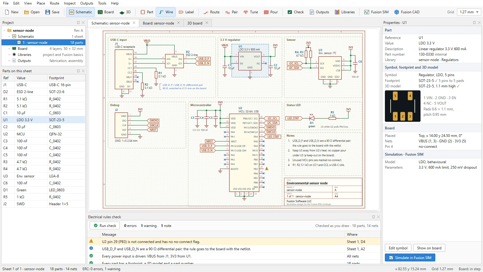
Design mockup: the schematic of a USB-C sensor board, with the regulator's footprint, 3D model and simulation model linked. Illustrative design.
Try it in Fusion SIM. Design it in Fusion EDA. Fit it in Fusion CAD.
Fusion EDA is board-level electronic design: schematic capture, libraries, PCB layout and manufacturing outputs in one product. It works with Fusion's simulation and mechanical products through recorded connections rather than file exports.
Fusion SIM tries circuits
Simulation for hobbyists, students and engineers checking an idea, from a quick schematic to a full analysis.fusionsim.cloud →
Fusion EDA designs boards
The schematic, parts, layout and manufacturing files of the board a product is built with.
Fusion CAD fits them
The enclosure and the board in one mechanical design, with the board's outline, holes and heights shared both ways.fusioncad.cloud →
Schematic capture that knows the board.
Draw circuits with parts that already know their footprint, 3D model and part number. Fusion EDA is planned to check the electrical rules as you draw, carry rules such as differential pairs and keep-outs from the schematic to the board, and build the bill of materials from the schematic.
Hierarchy and buses
PLANNEDSheets within sheets, buses and net labels, and reference designators numbered for you.
Electrical rules check
PLANNEDUnconnected pins, undriven power inputs and conflicting outputs, found as you draw and shown on the sheet.
Rules that reach the board
PLANNEDDifferential pairs, net classes and keep-outs set on the schematic become design rules on the board.
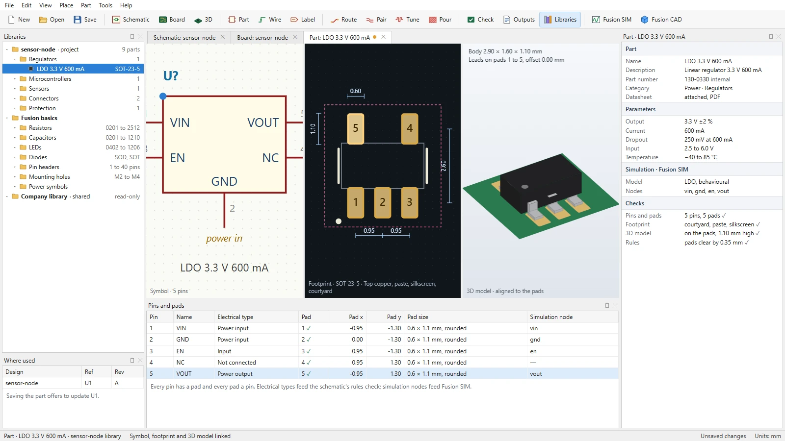
Every part with its symbol, footprint and 3D model.
A part in Fusion EDA is one record: the symbol you draw with, the footprint you place, the 3D model you check the fit with, its parameters and its part number. Pins are matched to pads in the part itself, so the schematic and the board cannot disagree about a connection.Design mockup: a regulator's symbol, its SOT-23-5 footprint and its 3D model, pin matched to pad. Illustrative part.
Symbols, footprints and 3D models
PLANNEDMade together and checked together: every pin has a pad, and the model sits on the footprint.
Common parts to start from
PLANNEDResistors, capacitors, LEDs, headers and mounting holes in standard sizes.
Shared company libraries
PLANNEDApproved parts with internal part numbers, shared by every design in the company.
Lay out and route the board.
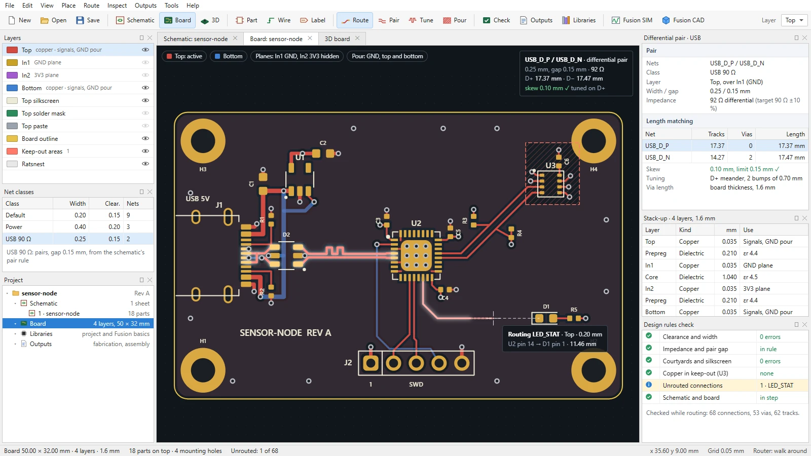
Set the stack-up and the design rules, place the parts, and route copper with a router that walks around obstacles or pushes them aside. Route differential pairs to an impedance computed from the stack-up, tune lengths to match, and pour copper, with the design rules checked as you go. The schematic and the board stay in step in both directions.Design mockup: routing a net on a 4-layer board, with the USB lines routed as a 90 Ω differential pair and tuned to match. The impedance and lengths were computed for this page from the mockup's geometry.
Stack-ups and design rules
PLANNEDLayers, materials and thicknesses, net classes, widths and clearances.
Interactive routing
PLANNEDWalk-around and push-and-shove routing, with vias placed as you change layers.
Differential pairs
PLANNEDPairs routed together at the width and gap that give their target impedance.
Length tuning
PLANNEDMeanders that match the lengths of pairs and buses, with vias counted.
Copper pours and planes
PLANNEDPoured areas and inner planes, with their clearances and keep-outs.
An autorouter
LATERAutomatic routing, after interactive routing is in place.
Designed with its enclosure in Fusion CAD.
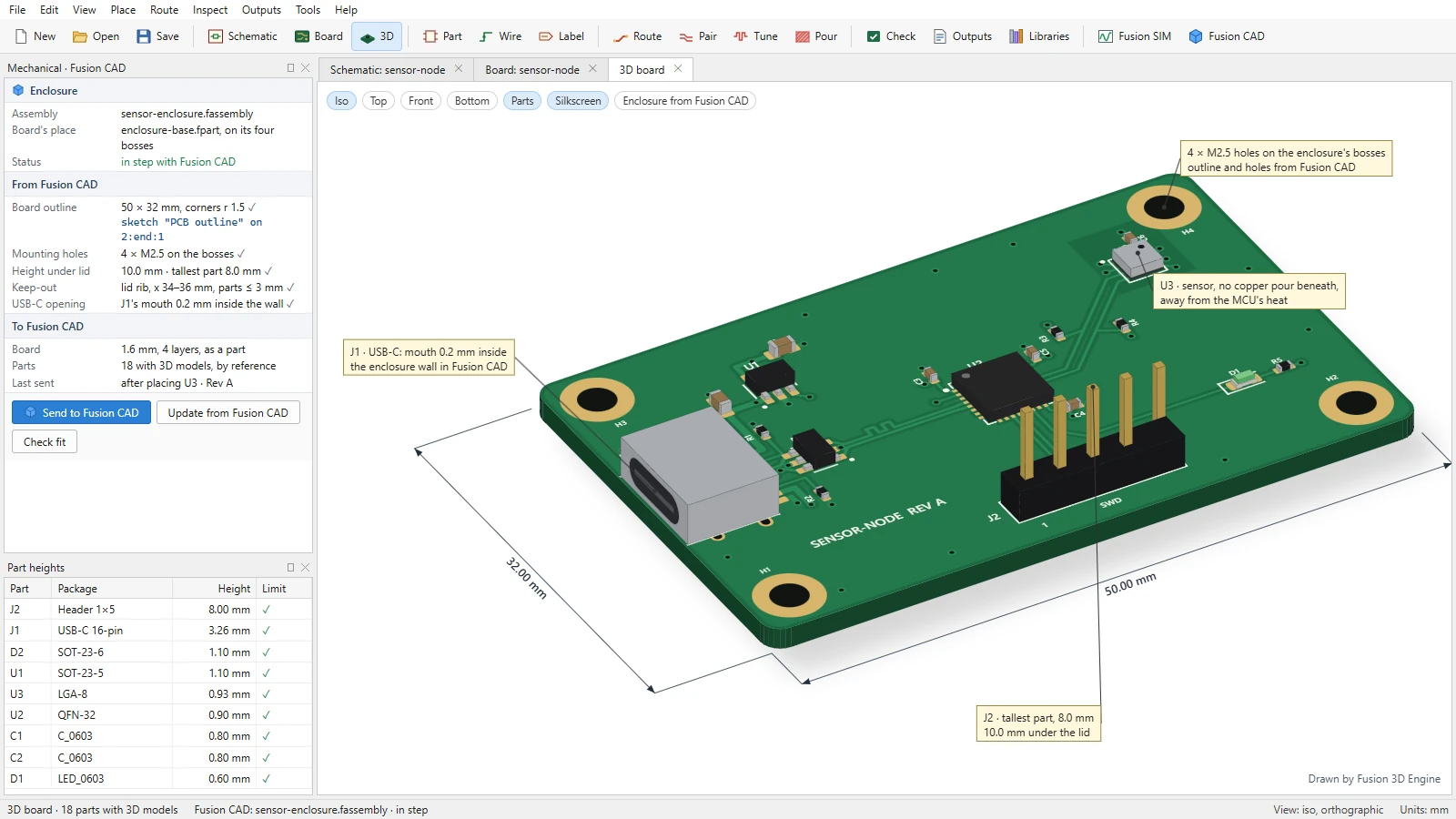
Fusion EDA is planned to show the board in 3D, drawn by Fusion 3D Engine, Fusion's core 3D engine. With Fusion CAD it is planned to share the board's outline, mounting holes, keep-outs and part heights in both directions, through a connection recorded in Fusion's shared contracts, so a board and its enclosure are designed together. Fusion CAD already reads boards from other tools' IDF files.Design mockup: the board in 3D, its outline and mounting holes from the enclosure in Fusion CAD. Illustrative data.
The board in 3D
PLANNEDParts with their 3D models over the solder mask, copper and silkscreen, drawn by Fusion 3D Engine.
Outline and holes from Fusion CAD
PLANNEDThe board's shape, mounting holes, keep-outs and height limits come from the enclosure's design.
The board back to Fusion CAD
PLANNEDThe board and its parts go to Fusion CAD, where the fit and clearances are checked.
Files for the board house and the assembler.
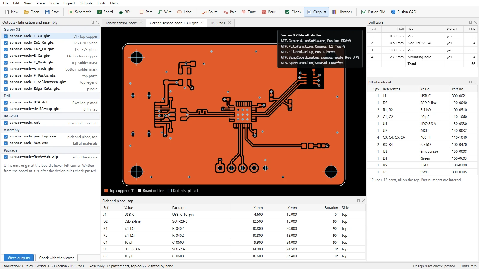
Fusion EDA is planned to write the manufacturing files from the board as it is: Gerber X2 with its file attributes, Excellon drill files, IPC-2581, and the pick-and-place and bill of materials files an assembler needs.Design mockup: the top copper layer as Gerber X2 with its file attributes, the drill table, the bill of materials and the pick-and-place list. Illustrative data.
Gerber X2 and drill files
PLANNEDEvery layer with its X2 attributes, and Excellon drill files with a drill map.
IPC-2581
PLANNEDThe whole board in one file: layers, stack-up, drills, parts and nets.
Assembly files
PLANNEDPick-and-place positions and the bill of materials, grouped by part.
One schematic with Fusion SIM.
Fusion SIM is where circuits are tried; Fusion EDA is where a product's board is designed. They are planned to share one schematic editor and one file format, so a circuit tried in Fusion SIM opens in Fusion EDA as the start of a real design, and a Fusion EDA design opens in Fusion SIM to be simulated. Nothing is redrawn.
Start in Fusion SIM
PLANNEDTry a circuit, then open the same schematic in Fusion EDA and carry on with footprints and a board.
Simulate from Fusion EDA
PLANNEDSend a design's circuit to Fusion SIM, which owns Fusion's circuit solvers.
RF and signal integrity
LATERFusion SIM's later RF and signal integrity modules, on the routed board.
Built in steps.
Fusion EDA is planned in C++ for Windows and Fusion OS, one step at a time, for board-level design.
1 · Schematic and libraries
PLANNEDSchematic capture, electrical rules, the bill of materials, and parts with their symbols, footprints and 3D models.
2 · Layout and outputs
PLANNEDStack-ups, design rules, placement, routing, copper pours, and Gerber X2, drill, IPC-2581 and assembly files.
3 · Fusion CAD
PLANNEDThe board's outline, holes, keep-outs and parts shared with Fusion CAD in both directions.
4 · Routing and Fusion SIM
PLANNEDPush-and-shove routing, differential pairs and length tuning, and simulation through Fusion SIM.
5 · And later
ROADMAPAn autorouter, and RF and signal integrity through Fusion SIM.
Board-level by design
SCOPEFusion EDA designs circuit boards. Designing the chips themselves is a different field and is not planned.
Part of the Fusion platform.
Fusion SIM
Fusion's simulation product, which owns the circuit solvers Fusion EDA designs are simulated with.fusionsim.cloud →
Fusion CAD
Fusion's mechanical design product, where boards meet their enclosures.fusioncad.cloud →
Fusion 3D Engine
Fusion's core 3D engine, which is to draw Fusion EDA's 3D board view.fusion3d.cloud →
Fusion EDA is planned.
Every screen on this page is a design mockup with illustrative data: the sensor board, its schematic, layout, impedance, lengths, drill counts and files were made for these mockups, not produced by Fusion EDA. Follow its progress, and the rest of the Fusion portfolio, on fusionsoftware.cloud.Visit fusionsoftware.cloudFusion EDA · Fusion Software LLC · 2026Fusion CADFusion SIMFusion MATFusion CAMFusion 3DFusion Software